Section Semiconductor Nanostructures
Section Semiconductor Nanostructures
Mission
Crystalline elements are crucial components of innovative technologies. As these technologies become increasingly smaller, it is essential that the dimensions of the crystalline structures decrease and that the crystallites are formed on the substrates in a very controlled manner. For this reason, it is the task of the Section Semiconductor Nanostructures to investigate the growth and local control of nano- and microcrystallites and to develop new methods for their implementation.
Research activities
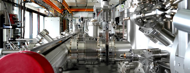
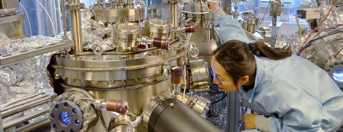
Low-dimensional growth concepts are beeing applied towards the use in novel technologies in this group. These comprise nanowire growth for new field-effect transistors, micro-island generation and thin-film growth from solution both for novel solar concepts as well as deposition of ultra-thin strained layers for the use in quantum computers. Not only technology development and characterization, but also concepts and realization of novel growth systems are in the focus. Within the framework of a Leibniz-funded project an MBE for the deposition of ultrapure 28Si layers is currently being developed and, in the course of a BMWi joint project, a CVD system for laser-assisted local nucleation processes is being built.
Head of section

Topics
Junior Research Group "SiGe-based Quantum Materials and Heterostructures"
The future potential of quantum technology and especially quantum computing is very high. SiGe heterostructures thereby constitute one of the most promising material platforms, since they combine high crystalline perfection and purity with potentially easy scalability, and the possibility to create a spin-neutral environment for quantum dots by isotopic enrichment.
The IKZ combines the competence and experience in processing isotopically enriched semiconductor materials such as 28Si, 72Ge, and 76Ge to supply high-quality quantum materials.
The research of our group focuses on the growth of SiGe-based heterostructures by molecular beam epitaxy (MBE) and their characterization for the application in quantum technology. We are specialized in nuclear spin-free SiGe/Si/SiGe and SiGe/Ge/SiGe heterostructures for spin qubits, as well as Si/SiO2 structures (Silicon on Insulator, SOI) for optical quantum emitters. The scientific interest centers upon obtaining preferably atomically flat interfaces, the realization of low dislocation densities, as well as the control of chemical impurities.
This work is funded by the Leibniz collaborative research project SiGeQuant and is shared with the partner institutes IHP (Frankfurt/Oder), IQI und ITH (RWTH Aachen), MPQ (Garching), as well as the Russian partners IPM RAS and University Nizhny.
Contact

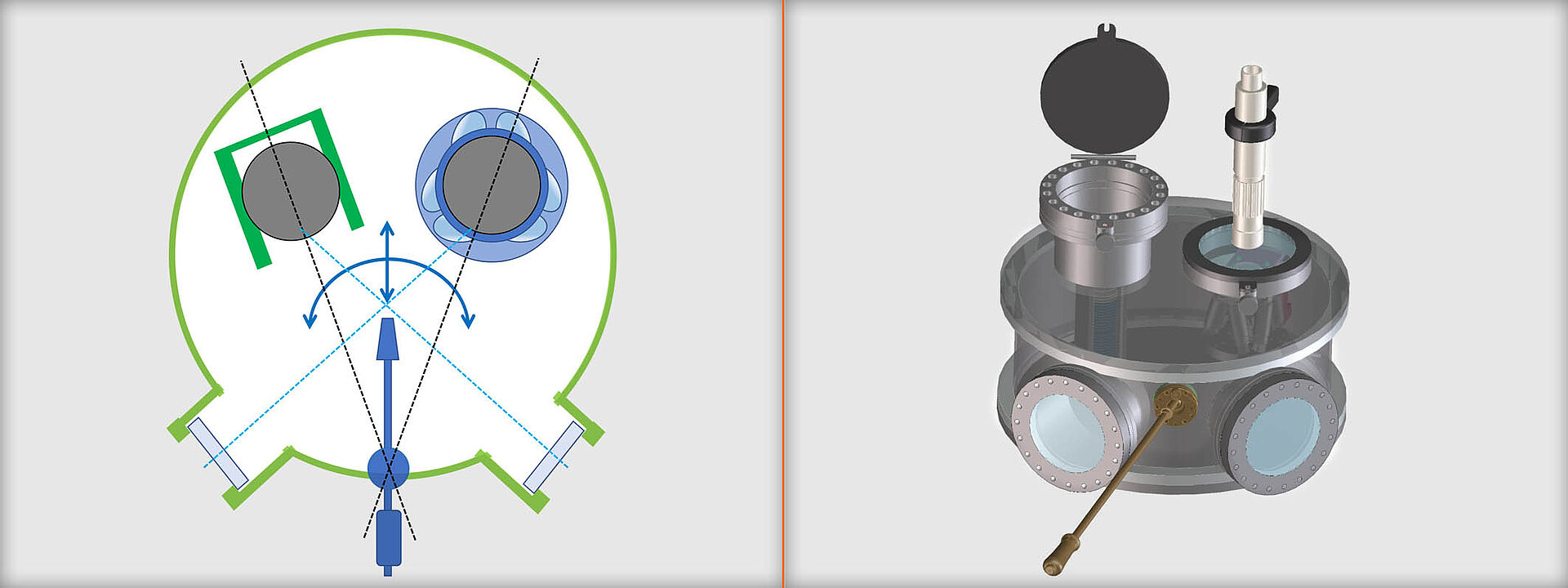
2D van der Waals materials and Layer Transfer
A new paradigm to assemble crystalline materials is established by layer transfer, a method to built-up novel epitaxial heterostructures which cannot be grown by traditional methods due to incompatibility of lattice parameters, symmetry, or others. We are aiming for a comprehensive and flexible technical approach to facilitate the realization of various demands in basic and applied research, seeking synergies with local academic and industrial partners.
We are currently setting up a layer transfer station in HV-conditions with the goal of a fully remote-controlled transfer process. We will transfer exfoliated monolayers of 2D-crystals and epitaxial films up to 2”-wafers. In basic research, a special interest is in emergent phases such as strongly correlated electronic matter in 2D-heterostructures. In applied research, high performance systems can be realized by the combination of the best materials for the best function in a hybrid approach.
Hao Chen, Pinjia Zhou, Jiawei Liu, Jiabin Qiao, Barbaros Oezyilmaz, Jens Martin
Gate controlled valley polarizer in bilayer graphene
Nature Communications
DOI: 10.1038/s41467-020-15117-y
Contact